- Home
- A-Z Catalogue
- Products
- Valves
- Cetop
- Manual Directional Valves
- Proportional Valves
- Poppet Valves
- High-Speed Linear Servo Valves
- All High-Speed Linear Servo Valves
- Cetop 10 (NG32) Two Stage Type High Speed Linear Servo Valves – LSVHG-10
- Cetop 10 (NG32) Two Stage Type High Speed Linear Servo Valves – LSVHG-10 (With Fail-Safe)
- Cetop 8 (NG25) Two Stage Type High Speed Linear Servo Valves – LSVHG-06
- Cetop 8 (NG25) Two Stage Type High Speed Linear Servo Valves – LSVHG-06 (With Fail-Safe)
- Cetop 7 (NG16) Two Stage Type High Speed Linear Servo Valves – LSVHG-04
- Cetop 7 (NG16) Two Stage Type High Speed Linear Servo Valves – LSVHG-04 (With Fail-Safe)
- Cetop 5 (NG10) Direct Type High Speed Linear Servo Valves – LSVG-03
- Cetop 5 (NG10) OBE Type Direct Operated Linear Servo Valves – LSVG-03-EH
- Cetop 3 (NG6) OBE Type Direct Operated Linear Servo Valves – LSVG-01-EH
- Pumps
- Pressure control
- Flow Control Valves
- Pressure Control Valves
- All Pressure Control Valves
- Brake Valves
- Direct Relief Valve
- Low Noise Solenoid Controlled Relief Valves
- Low Noise Pilot Operated Relief Valves
- Pilot Operated Relief Valves
- Pressure reducing and relieving valves
- Pressure reducing and check valves
- Pressure control valves
- Remote Control Relief Valves
- Solenoid Controlled Relief Valves – BSG
- Solenoid Controlled Relief Valves – BST
- Unloading relief valves
- Check valves
- Environmental
- Valves
- Hydraulic Systems
- Power pack
- About Us
- Contact
- Blog

What Is Flip Chip Packaging and How Does It Work?
Flip Chip Packaging places a semiconductor die face down on a substrate. Tiny solder bumps or copper pillars create direct electrical and mechanical connections. Unlike traditional wire bonding, this approach shortens the signal path. It can also improve electrical performance, thermal transfer, and package density. The process begins with bump formation and wafer testing. The die is then aligned over matching substrate pads. Precision matters. A small placement error can weaken hundreds of connections.
John H. Lau, a widely recognized semiconductor packaging expert, has stated, “Flip chip technology is a key enabling technology for high-performance electronic products.” His view reflects the technology’s role in processors, graphics devices, networking hardware, and advanced sensors. During assembly, controlled heating reflows the solder joints. Underfill material often fills the narrow gap beneath the die. It reduces stress caused by different material expansion rates. Inspection may include X-ray imaging, electrical testing, and thermal evaluation.
The method is powerful, but it is not automatically better in every design. Warpage, voids, contamination, and uneven underfill can reduce reliability. Engineers must balance cost, substrate choice, heat removal, and repair difficulty. That balance deserves closer attention. This article explains how Flip Chip Packaging works, from bump creation to final testing. It also examines common materials, manufacturing stages, advantages, limitations, and practical reliability concerns. Some details vary by application. A mobile processor, automotive controller, and high-power module may require very different package structures. Understanding those differences prevents overly simple conclusions. Even a well-designed package can fail when production control is weak.
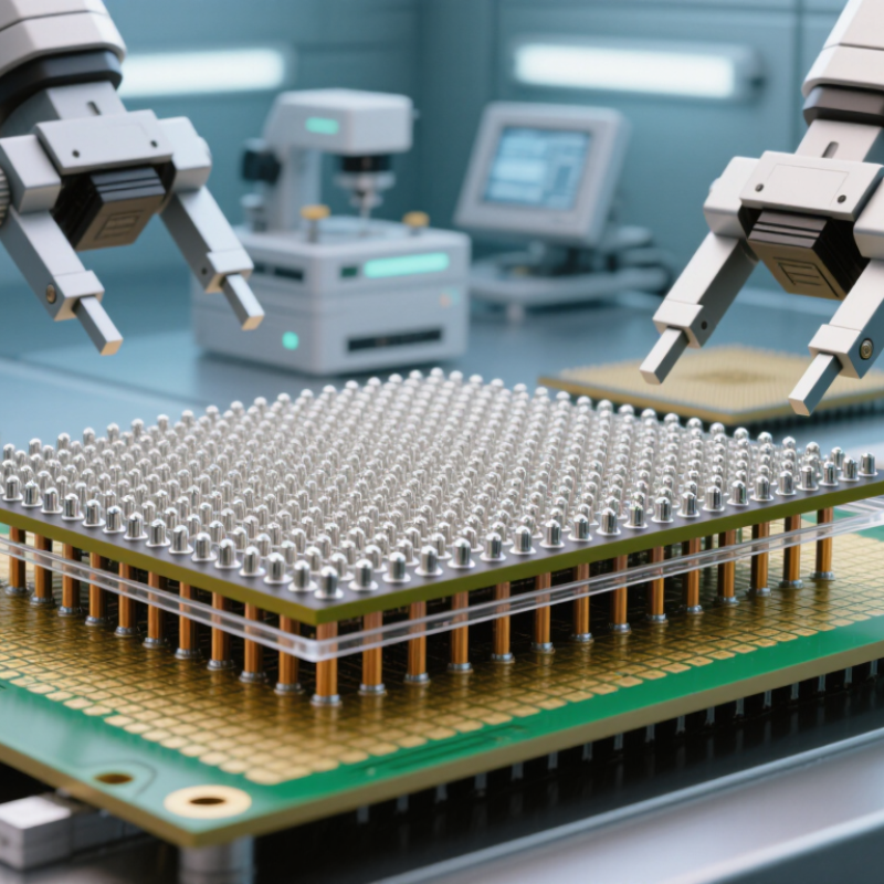
Table of Contents [Hide]
Flip Chip Packaging: Direct Die-to-Substrate Interconnection with 100–2,000+ I/Os
Flip chip packaging connects a silicon die directly to a substrate through solder bumps or copper pillars. The die is flipped, so its active surface faces the substrate. This short path supports dense electrical routing and reduces package resistance. In advanced designs, 100 to more than 2,000 I/Os can fit beneath one die. That density matters for processors, memory devices, and high-speed signal systems.
During assembly, engineers place bumps on matching substrate pads with precise alignment. Controlled heating forms reliable joints, while underfill spreads stress beneath the die. Inspection commonly checks bump height, voids, alignment, and connection continuity. From practical failure analysis, tiny alignment errors can become expensive electrical defects. Heat also travels through a shorter route, but thermal limits still require careful design. A compact interconnect does not automatically solve cooling problems.
The substrate must manage power delivery, signal integrity, and mechanical expansion at once. Design teams simulate impedance, current density, warpage, and thermal cycling before production. They also test samples through temperature changes and repeated operating loads. One limitation deserves attention: repair is difficult after the die is attached. Yield can suffer when thousands of joints must perform consistently. The design is powerful, but not forgiving. Unexpected warpage or uneven underfill can still undermine an otherwise advanced package.