- Home
- A-Z Catalogue
- Products
- Valves
- Cetop
- Manual Directional Valves
- Proportional Valves
- Poppet Valves
- High-Speed Linear Servo Valves
- All High-Speed Linear Servo Valves
- Cetop 10 (NG32) Two Stage Type High Speed Linear Servo Valves – LSVHG-10
- Cetop 10 (NG32) Two Stage Type High Speed Linear Servo Valves – LSVHG-10 (With Fail-Safe)
- Cetop 8 (NG25) Two Stage Type High Speed Linear Servo Valves – LSVHG-06
- Cetop 8 (NG25) Two Stage Type High Speed Linear Servo Valves – LSVHG-06 (With Fail-Safe)
- Cetop 7 (NG16) Two Stage Type High Speed Linear Servo Valves – LSVHG-04
- Cetop 7 (NG16) Two Stage Type High Speed Linear Servo Valves – LSVHG-04 (With Fail-Safe)
- Cetop 5 (NG10) Direct Type High Speed Linear Servo Valves – LSVG-03
- Cetop 5 (NG10) OBE Type Direct Operated Linear Servo Valves – LSVG-03-EH
- Cetop 3 (NG6) OBE Type Direct Operated Linear Servo Valves – LSVG-01-EH
- Pumps
- Pressure control
- Flow Control Valves
- Pressure Control Valves
- All Pressure Control Valves
- Brake Valves
- Direct Relief Valve
- Low Noise Solenoid Controlled Relief Valves
- Low Noise Pilot Operated Relief Valves
- Pilot Operated Relief Valves
- Pressure reducing and relieving valves
- Pressure reducing and check valves
- Pressure control valves
- Remote Control Relief Valves
- Solenoid Controlled Relief Valves – BSG
- Solenoid Controlled Relief Valves – BST
- Unloading relief valves
- Check valves
- Environmental
- Valves
- Hydraulic Systems
- Power pack
- About Us
- Contact
- Blog

How to Build a 555 Timer Circuit?
A 555 timer is a small, versatile integrated circuit that can turn a few basic components into a flashing LED, pulse generator, or simple delay. Building a 555 Ic Timer Circuit is a practical way to learn how resistors and capacitors shape an electronic signal. The parts are familiar: a 555 chip, a breadboard, jumper wires, an LED, a current-limiting resistor, and a timing capacitor. Start with a blink.
This introduction focuses on the common astable configuration, where the timer repeatedly switches its output on and off. You will learn what each important pin does, how to connect the timing components, and how to estimate the flash rate. The familiar timing formula is a useful starting point, not a promise of perfect accuracy. Component tolerances, wiring, and the specific 555 variant can all affect the result.
Small details matter. Check the pin-one mark before placing the chip, observe the LED’s polarity, and confirm the supply voltage against the datasheet for your exact device. Disconnect power before changing breadboard connections. Then test the circuit and compare its actual timing with your estimate. It may blink too quickly. That is useful evidence, not failure: measure the result, review the component values, and adjust one part at a time. A first build can feel untidy, and the explanation may not answer every question. Careful observation makes the next revision clearer and more reliable.
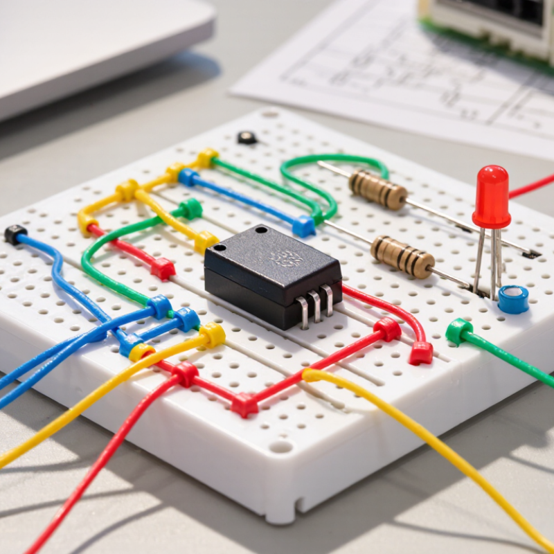
Table of Contents [Hide]
Understanding the 555 Timer and Its Operating Modes
A 555 timer is an eight-pin integrated circuit that changes its output when capacitor voltage crosses internal thresholds. Inside, comparators control a latch, while a discharge transistor helps charge or empty the timing capacitor. That simple arrangement supports several useful operating modes. A pinout diagram helps prevent wiring mistakes.
Monostable mode produces one timed pulse after a trigger. A resistor and capacitor set its approximate duration; component tolerances can shift the result.
Astable mode repeatedly switches between high and low, creating a square wave. Two resistors and one capacitor set its timing, though the high and low periods may differ.
Bistable mode acts like a basic set-reset latch. A brief input can change its output, which stays put until another input arrives.
When assembling a circuit, check the pin connections and supply-voltage limits in the specific device’s datasheet. Place a small bypass capacitor near the supply pins to reduce unwanted switching noise. Keep timing leads short, especially around the capacitor.
Small detail.
A common bench mistake is choosing a capacitor without considering leakage or tolerance. I still find it useful to measure the actual timing, rather than trusting a calculation alone. A simple LED can show the output changing, but its resistor must limit current.